By introducing defects into the perfect surface of graphene on silicon carbide, researchers at LiU have increased the capacity of the material to store electrical charge. This result, which has been published in the scientific journal Electrochimica Acta, increases our knowledge of how this ultrathin material can be used.
The thinnest material ever produced, graphene, consists of a single layer of carbon atoms. They form a chicken-wire structure one atom thick, with unique properties. It is around 200 times stronger than steel, and highly flexible. It is transparent, but gases and liquids cannot pass through it. In addition, it is an excellent conductor of electricity. There are many ideas about how this nanomaterial can be used, and research into future applications is intense.
“Graphene is fascinating, but extremely difficult to study,” says Mikhail Vagin, principal research engineer at the Department of Science and Technology and the Department of Physics, Chemistry and Biology at Linköping University.
One of the factors contributing to the difficulty in understanding the properties of graphene is that it is what is known as an “anisotropic” material. This means that its properties when measured on the plane surface of the carbon atom layer differ from those measured at the edges. Furthermore, attempts to understand the behaviour of graphene at the atomic level are complicated by the fact that it can be produced in several ways. The properties of graphene in small flakes, which have many edges, differ in several ways from those of graphene produced as sheets with an area around 1 cm2.
Read more at Linköping University
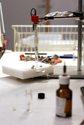
Image: Instruments to monitor graphene anodization (Credits: Linköping University)


