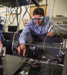
Next-generation solar cells made of super-thin films of semiconducting material hold promise because they’re relatively inexpensive and flexible enough to be applied just about anywhere.
Researchers are working to dramatically increase the efficiency at which thin-film solar cells convert sunlight to electricity. But it’s a tough challenge, partly because a solar cell’s subsurface realm—where much of the energy-conversion action happens—is inaccessible to real-time, nondestructive imaging. It’s difficult to improve processes you can’t see.
Now, scientists from the Department of Energy’s Lawrence Berkeley National Laboratory (Berkeley Lab) have developed a way to use optical microscopy to map thin-film solar cells in 3-D as they absorb photons.


